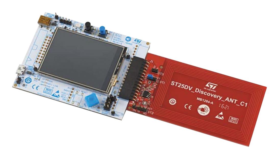
ST ST25DV Discovery, MB1283 version
Overview
The ST25DV04K device is a dynamic NFC/RFID tag IC with a dual interface. It embeds a 4 Kbits EEPROM memory. It can be operated from an I2C interface, or by a 13.56 MHz RFID reader, or by a NFC phone. The ST25DV04K Class 5 antenna daughter card, included in the kit, can be replaced by Class 1 or Class 6 antennas.
The ST25DV-DISCOVERY is a demonstration kit to evaluate the features and capabilities of the ST25DV series. It is based on the NFC ST25DV04K device embedded on a daughter card using a Class 5 antenna and a STM32 processor driving a mother board.

Note
The ST25DV itself is not implemented yet.
Hardware
The ST25DV Discovery kit provides the following hardware components:
Main board: ST25DV_Discovery_Mboard:
STM32F405VGT6 LQFP100 32-bit microcontroller, with 1 Mbyte Flash memory, 192 + 4 Kbytes SRAM.
LCD color screen (320 x 200 pixels)
Touch screen driver
Different color LEDs (power, user, ST link)
User push button
Joystick for menu selection
Reset button
On board ST link for microcontroller firmware upgrade and debug
ST link mini USB
User micro USB
USB micro or mini connector for board powering
Demonstration edition (optional add-on module) with Bluetooth Low Energy module, Wi-Fi ® module and JTAG 20 pin connector
It exists in two variants, MB1283 and MB1285.
Antenna daughter board: ST25DV_Discovery_ANT_C5:
40 mm x 24 mm, 13.56 MHz inductive antenna etched on the PCB
ST25DV04K Dynamic NFC / RFID tag
I 2 C interface connector
Energy harvesting output (VOUT) with a 10nF capacitance filtering circuit
GPO configurable as RF WIP/BUSY output, to indicate that an RF operation is ongoing
The antenna board can be removed, and its 14-pin 0.254mm header connector used as an eval kit header.
Connections and IOs
Default Zephyr Peripheral Mapping
UART_6 TX/RX : PC6/PC7 (ST-Link Virtual Port Com)
UART_2 TX/RX : PA2/PA3 (Available on J6 connector)
I2C1 SCL/SDA : PB6/PB7 (Touchscreen STMPE811, interrupt pin PB5)
SPI2 SCK/MOSI/CS : PB13/PC3/PB12 (LCD display FRD24048TP, reset pin PC1, DC pin PC0)
SPI1 SCK/MISO/MOSI/CS : PA5/PA6/PA7/PA4 (External ST25DV connector J6)
GPIO : PE8/PE9/PE10/PE11/PE12 (Joystick)
LD1 : PC13 (Orange led)
LD2 : PC4 (Yellow led)
GPIO : PE15/PE7 (Available on external ST25DV connector J6)
GPIO : PE14 (Available on J5 connector)
Serial Port
The Zephyr console output and shell are assigned to UART6, which is connected to the onboard ST-LINK/V2 Virtual COM port interface. Default communication settings are 115200 8N1.
Programming and Debugging
Applications for the st25dv_mb1283_disco board configuration can be built and
flashed in the usual way (see Building an Application and
Run an Application for more details).
If programming fails, press the reset button (black) and release it while “west flash” is running.
Flashing
ST25DV Discovery kit includes an ST-LINK/V2 embedded debug tool interface. This interface is supported by the openocd version included in the Zephyr SDK.
Flashing an application to ST25DV Discovery
First, connect the ST25DV Discovery kit to your host computer using the USB port to prepare it for flashing. Then build and flash your application.
Here is an example for the Hello World application.
# From the root of the zephyr repository
west build -b st25dv_mb1283_disco samples/hello_world
west flash
Run a serial host program to connect with your board:
$ minicom -D /dev/ttyACM0
You should see the following message on the console:
Hello World! st25dv_mb1283_disco
Debugging
You can debug an application in the usual way. Here is an example for the Hello World application.
# From the root of the zephyr repository
west build -b st25dv_mb1283_disco samples/hello_world
west debug
